1) General Specifications
Screen Size
7.0 inch (portrait)
Technology
AMOLED (LTPS)
Resolution
1080 (W) × 1920 (H)
Active Area
87.1344 (H) × 154.9056 (V) mm
Pixel Density
315 PPI
Pixel Layout
V-style4
Touch
On-Cell, FT3519
Display IC
ICNA3512
Frame Rate
60 / 90 / 120 / 144 Hz (configurable)
Module Outline
89.1344 × 160.9056 × 1.028 mm
Interface
MIPI DSI 4-Lane + TE
Compliance
RoHS 2.0
Note: This article consolidates the PDF “7.0INCH AMOLED Module (Vertical type).pdf” Rev.V1.
2) IO Terminals & Pin Assignment
2.1 Main FPC — OK-F302-39115
#
Signal
I/O
Description
1-3,9,12,15,18,21,24,27,32
GND
P
Ground
4-8
VBAT
P
EL PMIC power (4.0-4.8 V, typ 4.2 V)
10,11,39
NC
/
No connect
13,14
D3P/D3N
I
MIPI Data Lane 3
16,17
D0P/D0N
I/O
MIPI Data Lane 0
19,20
CLKP/CLKN
I
MIPI Clock
22,23
D1P/D1N
I
MIPI Data Lane 1
25,26
D2P/D2N
I
MIPI Data Lane 2
28
RST
I/O
Display reset
29
VDDI
P
Logic power (1.65-1.95 V, typ 1.8 V)
30
VCI
P
Analog power (2.65-3.60 V, typ 3.0 V)
31
TE
O
Tearing effect sync
33
TP_AVDD
P
Touch analog power (2.7-3.6 V)
34
TP_DVDD
P
Touch digital power (1.7-3.6 V)
35,36
TP_SDA/TP_SCL
I/O,I
Touch I²C
37
TP_RESET
I
Touch reset
38
TP_INT
I
Touch interrupt
Legend: I = Input, O = Output, P = Power, I/O = Bidirectional.
2.2 System Interface Topology
VBAT → EL PMIC         VDDI (1.8 V) → DDIC logic     VCI (3.0 V) → DDIC analog
MIPI DSI 4-Lane → ICNA3512           TE → Host sync
Touch: FT3519 via I²C (SCL/SDA) + INT + RESET
3) Absolute Maximum Ratings
Item
Symbol
Min
Max
Unit
Note
Logic Supply
VCI
-
3.6
V
Do not exceed
Analog Supply
VDDIO
-
3.6
V
Per doc naming
PMIC Supply
VBAT
-
7.0
V
Absolute max
Operating near or over absolute maxima can cause permanent damage and reduce reliability.
4) Electrical Characteristics
Item
Symbol
Min
Typ
Max
Unit
Logic Supply
VDDI
1.65
1.80
1.95
V
Analog Supply
VCI
2.65
3.00
3.60
V
Default VBAT
VBAT
4.0
4.2
4.8
V
Input VIH
VIH
0.70×VDDI
-
VDDI
V
Input VIL
VIL
0
-
0.30×VDDI
V
Output VOH
VOH
0.80×VDDI
-
VDDI
V
Output VOL
VOL
0
-
0.20×VDDI
V
Current and power measured at white pattern, 25 °C.
5) AC Characteristics
5.1 MIPI DSI
Supports 4-lane HS burst. Follow ICNA3512 D-PHY timing for LP↔HS transitions, setup and hold, eye margins, and skew.
5.2 RESET Timing
At VDDI = 1.65-1.95 V, VCI = 2.65-3.6 V, -40 to 85 °C: hold RST = Low ≥10 ms, then High ≥20 ms before DSI init.
6) Recommended Power On/Off Sequence
6.1 Power-On
Enable VDDI → VCI → VBAT with 2-5 ms inter-rail delays.
RST = Low (≥10 ms) → High (≥20 ms).
Configure MIPI, send init table, set gamma, brightness, and frame rate.
6.2 Power-Off
Display OFF , wait frame end.
Disable VBAT → VCI → VDDI .
Ensure DSI returns to LP before rails drop.
// Pseudo code
enable(VDDI); delay_ms(2);
enable(VCI);  delay_ms(2);
rst_low();    delay_ms(10);
rst_high();   delay_ms(20);
mipi_init(4_lanes, clk_hz);
dsi_write_seq(init_table);
set_gamma(2.2);
set_brightness(nits_to_code(300));
set_fps(120);
dsi_cmd(DISPLAY_ON);
7) Touch Design
7.1 Matrix and Pattern
Structure: On-Cell, diamond pattern, 2T1R
Channels: Tx = 20 / Rx = 36
Pitch: Tx 4.359 mm / Rx 4.3042 mm
7.2 Power
TSP_AVDD: 2.8 / 3.0 / 3.3 V (2.7-3.6 V)
TSP_VDDIO: 1.8 V default (1.7-3.6 V or same as AVDD)
7.3 Touch FPC (10-pin)
#
Signal
Description
1
GND
Ground
2
TSP_AVDD
Touch analog power
3
TSP_VDDIO
Touch digital power
4
TSP_INT
Touch interrupt
5
TSP_SDA
I²C data
6
TSP_SCL
I²C clock
7
TSP_RESET
Touch reset
8
TSP_VSYNC
Display VSYNC (sync)
9
NC
No connect
10
GND
Ground
Use 4.7 kΩ pull-ups on SDA/SCL. Place ESD TVS near the connector. Keep I²C away from MIPI and PMIC traces.
Reference BOM (excerpt)
C1-C4: 1 µF / 6.3 V / 0402; C5: 1 µF / 16 V / 0402; C6: 1 µF / 10 V / 0402
D1: TVS 5 V / 0402; D2: TVS 3.3 V / 0402
U1: FT3519
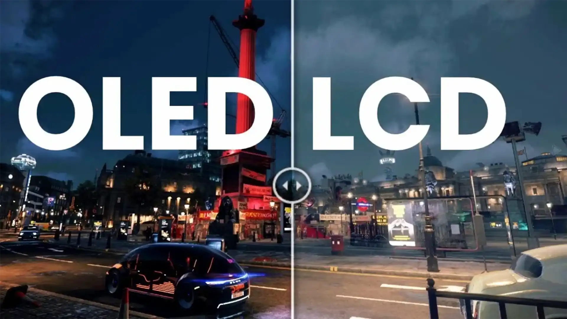
8) Optical Characteristics
Item
Condition
Min
Typ
Max
Unit
Note
Viewing Angle (U/D/L/R)
CR ≥ 20000
80
-
-
deg
Symmetric
Contrast Ratio
θ = 0°
100,000
-
-
-
CS2000A
White CIE (x,y)
Center
0.290/0.296
0.310/0.316
0.330/0.336
-
CIE1931
Red (x,y)
Center
0.652/0.285
0.682/0.315
0.712/0.345
-
-
Green (x,y)
Center
0.200/0.676
0.240/0.716
0.280/0.756
-
-
Blue (x,y)
Center
0.108/0.016
0.138/0.046
0.168/0.076
-
-
Luminance Uniformity
9-point
75
-
-
%
Lmin/Lmax
NTSC Coverage
-
100
-
-
%
Nominal
Luminance (Normal)
White
720
800
880
cd/m²
CS2000A
Luminance (HBM)
White
900
1000
1100
cd/m²
CS2000A
Flicker
G127 / 60 Hz / 800 nits
-
-30
-
dB
CA410 JEITA
Crosstalk
-
-
2
-
%
-
Response Time
25 °C
-
-
2
ms
TON/TOFF
Gamma
Gray16-240
2.0
2.2
2.4
-
-
Dark room center measurement at 25 °C. Equipment: CS2000A / CA410.
9) Environmental / Reliability
#
Test
Condition
Standard
1
High-Temp Operation
+70 °C, 120 h
IEC 62341-5:2009
2
Low-Temp Operation
-20 °C, 120 h
IEC 62341-5:2009
3
High-Temp Storage
+80 °C, 120 h
IEC 62341-5:2009
4
Low-Temp Storage
-40 °C, 120 h
IEC 62341-5:2009
5
Thermal Shock
-40 ↔ +80 °C, 30 min dwell, 30 cycles
IEC 62341-5:2009
6
HTHH Operation
60 °C, 90%RH, 120 h
IEC 62341-5:2009
10) Appearance & Quality
10.1 Defect Classes
CR (Critical) : Safety or complete functional loss.
MA (Major) : Function degraded or partial loss, or three or more Minor combined.
MI (Minor) : Cosmetic, with no functional impact.
10.2 Sampling and AQL
Sampling: GB/T 2828.1-2012 (normal inspection)
AQL: CR = 0; MA = 0.65; MI = 1.0
10.3 Inspection Conditions
Unlit 1000 ± 200 lux; lit ≤ 200 lux; black background.
Distance 30 ± 5 cm; Angle ±45°.
Time: unlit 10-12 s; lit 1-3 s per pattern; 15-35 °C, 20-75%RH.
10.4 Typical Cosmetic Criteria (excerpt)
Bright dots and lines: Not allowed.
Dark dot: D ≤ 0.15 mm ignore; D > 0.15 mm NG.
Foreign dots: D ≤ 0.15 mm and DS ≥ 30 mm ignore; 0.15 < D ≤ 0.20 with N ≤ 2 and DS > 50 mm OK; D > 0.20 mm NG.
Line scratch: W ≤ 0.03 and L ≤ 5 and DS ≥ 10 ignore; 0.03 < W ≤ 0.05 and L ≤ 2 ignore; 2 < L ≤ 5 N ≤ 4; L > 5 or W > 0.5 NG.
POL overflow: W ≤ 0.2 mm ignore; W > 0.2 mm NG.
Glass chipping: zone-based PAD, Bonding, and OA limits per drawing.
11) Mechanical & Packaging
11.1 Key Mechanical Notes
Module thickness 1.028 mm (including POL and foam). Local stack-ups must meet drawing Hmax.
Connectors: Main FPC OK-F302-39115 ; Touch FPC OK-F501-10325 .
Tear tabs, tapes, and foams per drawing must not intrude AA.
11.2 Packing
Tray surface resistivity 10⁴-10⁹ Ω; 4 pcs/tray.
Carton: 24 trays (22 full + 2 empty PET trays) → 88 pcs/carton.
12) Precautions for Use
Glass module: avoid drop and impact; do not press the screen or edges.
POL surface is soft; blow first then dry-wipe; if solvent is needed use ethyl alcohol only .
No water, ketone, or aromatic solvents. Do not disassemble.
Do not feed signals when logic power is off. Ensure ESD control and avoid overly dry environments.
Peel protective film slowly with ESD grounding.
Storage: 0-40 °C, ≤80%RH, no acid, alkali, or harmful gas, avoid light. Transport: prevent drop, pressure, wet exposure, and sun exposure.
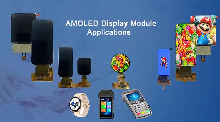
13) Applications & Recommendations
13.1 Consumer and Premium Handhelds
Android handheld consoles: portrait 7-inch format works well for indie and retro usage; 120/144 Hz reduces blur.
High-end e-book and note devices: 315 PPI supports crisp text; HBM 1000 nits improves visibility.
Smart home panels: premium contrast and flicker control support comfortable viewing.
13.2 Industrial HMI and Rugged Terminals
Factory and UAV ground stations: operating range supports outdoor deployment needs.
Medical and diagnostic carts: wide viewing angle helps multi-person review.
Retail POS and kiosks: HBM performance helps in bright spaces.
13.3 Automotive and Mobility
Rear-seat systems: deep blacks and 120 Hz improve perceived quality.
Cluster-adjacent widgets: On-Cell touch reduces total stack height.
Fleet tablets: low-temperature start and protected logistics handling support field use.
13.4 Public Information and Hospitality
Room signage: high contrast and good uniformity create a premium appearance.
Museum labels: OLED blacks work well in dim rooms.
Airports and stations: HBM improves visibility in bright halls.
13.5 Pro AV and Photography
Field monitors: high contrast supports focus and visual review.
Wireless mixer interfaces: TE and high refresh help reduce visible artifacts.
13.6 Education and Remote Work
Podium secondary screens: portrait layout suits notes and timers.
Portable conference terminals: wide view and low flicker support long sessions.
13.7 Integration Tips
EMI and ESD: keep MIPI pairs short and length-matched; place TVS near the FPC.
Thermal: couple PMIC to chassis and avoid AA-edge hot spots.
Power: enforce sequencing and budget for HBM and high-fps current peaks.
Touch: respect FT3519 reset and INT timing; keep I²C away from noisy regions.
Quality: inspect under the specified lighting conditions to catch subtle defects.
14) FAQ
1) What is the correct power-on order for this AMOLED module?
VDDI → VCI → VBAT → RESET High → DSI init → Display ON
Hold RST = Low ≥10 ms after rails are stable, then High ≥20 ms.
Configure MIPI and push the init table before enabling display output.
Power-off: Display OFF → VBAT → VCI → VDDI .
// Quick sketch
enable(VDDI); delay_ms(2);
enable(VCI);  delay_ms(2);
rst_low();    delay_ms(10);
rst_high();   delay_ms(20);
mipi_init(4_lanes, clk);
dsi_write_seq(init_table);
dsi_cmd(DISPLAY_ON);
2) How many MIPI lanes are supported? What about TE?
Up to 4-Lane MIPI DSI in HS burst.
TE is available for frame sync and tearing mitigation.
3) What are the power rails and typical voltages?
Rail
Nominal
Range
Purpose
VDDI
1.8 V
1.65-1.95 V
DDIC logic
VCI
3.0 V
2.65-3.60 V
DDIC analog
VBAT
4.2 V
4.0-4.8 V (max abs 7 V)
EL PMIC / emission
TSP_AVDD
2.8 / 3.0 / 3.3 V
2.7-3.6 V
Touch analog
TSP_VDDIO
1.8 V
1.7-3.6 V
Touch logic
4) What brightness and flicker can I expect?
800 cd/m² typical, 1000 cd/m² HBM.
Uniformity ≥75% (9-point).
Flicker ≤ -30 dB at Green127, 60 Hz, 800 nits.
5) What is the supported temperature range?
Operation: -20 °C to +70 °C
Storage: -40 °C to +80 °C
Thermal shock tested per IEC 62341-5.
6) Does it support high refresh like 120/144 Hz?
Yes. Ensure MIPI bandwidth, proper init scripts, synced TE and VSYNC, and sufficient power budget at high frame rates.
7) How should the touch controller be wired and protected?
I²C with 4.7 kΩ pull-ups.
TVS at the connector; keep I²C away from MIPI and PMIC areas.
Respect reset and INT timing.
8) Any mechanical or packing cautions?
Hmax limits in the drawing must be respected at FPC, steel, and IC areas.
Tray ESD 10⁴-10⁹ Ω; 4 pcs/tray; 88 pcs/carton.
9) How should cosmetic inspection be performed?
Unlit 1000 ± 200 lux; lit ≤ 200 lux; distance 30 ± 5 cm; ±45° viewing.
Bright dots and lines NG; dark dot D ≤ 0.15 mm OK; > 0.15 mm NG.
Use ND 6% for Mura, gauges for coverage, microscope 20-50×.
AQL: CR = 0; MA = 0.65; MI = 1.0.
10) Suitable application scenarios?
Handheld consoles, premium e-readers, smart home panels.
Industrial HMI, medical carts, POS and kiosks.
Rear-seat entertainment, dash-adjacent widgets.
Public information signage and Pro AV field monitors.
11) Any ESD, EMI, and power tips?
Use short, matched MIPI lanes and correct impedance; place TVS near FPC.
Follow strict power sequencing and budget for HBM and fps peaks.
Thermally couple the PMIC and avoid AA-edge hot spots.
12) Which solvents are safe?
Only ethyl alcohol is allowed for the POL surface. Water, ketones, and aromatics are prohibited.
13) How should the protective film be handled?
Peel slowly with ESD grounding. Peeling can generate static that is hazardous to OLED and IC devices.
14) How should optical measurements be taken?
Use a dark room, center point, 25 °C.
Use CS2000A for luminance, contrast ratio, and CIE; CA410 for flicker and gamma.
Uniformity should be measured on a 3×3 grid.
15) Is high-humidity operation supported?
Qualified at 60 °C, 90%RH, 120 h under IEC 62341-5. Even so, design for moisture barriers and avoid condensation.
VIDEO


コメントを書く
このサイトはhCaptchaによって保護されており、hCaptchaプライバシーポリシーおよび利用規約が適用されます。