
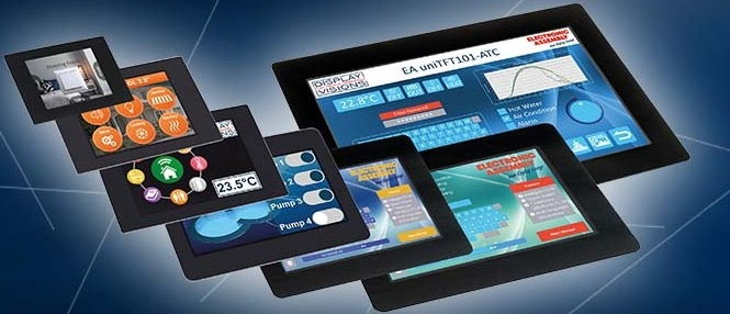
This article explains how TFT LCD modules are made and how the main parts come together in the final product. A typical TFT module includes the LCD cell, color filter, driver and control circuits, a PCB, connection parts such as FPC or metal leads, a backlight unit, and supporting mechanical parts such as the frame and rear cover. Each part has a specific role, and the final display performance depends on how well these parts are designed, processed, and assembled. The following sections look at the module structure, the main production stages, and the film and cell processes used in TFT LCD manufacturing.

The structure of TFT LCD display
TFT-LCD technology has become one of the main display technologies used in consumer, industrial, and automotive products. It is widely used in TVs, computer monitors, laptops, handheld devices, navigation systems, cameras, and smartphones.
TFT-LCD development started decades ago and has continued to improve with advances in materials, process control, and panel design. Early TFT work used compound semiconductors such as CdSe, but silicon-based processes later became more suitable for large-scale manufacturing. Today, amorphous silicon (A-Si) and low-temperature polysilicon (LTPS) are commonly used because they fit the temperature limits of glass substrates and can be produced at scale.
Several LCD modes are used in the market, including TN, IPS, and VA-related structures. In this article, the focus is mainly on the standard TFT-LCD module structure and the production flow behind it.
A TFT-LCD display module usually includes the following parts:
- Liquid Crystal Panel: The main display section that forms the image. It is built from two glass substrates with a liquid crystal layer in between.
- Polarizers: Installed on both sides of the panel to control the light passing through the liquid crystal layer.
- Color Filter: Used to generate color by defining red, green, and blue sub-pixels.
- TFT Array: The active matrix that drives each pixel.
- Backlight: The light source behind the panel that makes the image visible.
- Drive Circuit: Handles input signals and controls the panel and backlight.
When these parts are combined, they form a complete TFT-LCD module. The image seen by the user depends on the electrical control of the TFT array and the way the liquid crystal layer modulates light from the backlight.

The manufacturing process of TFT LCD displays
The manufacturing flow of a TFT display is usually divided into four main sections: TFT array, color filter, cell, and module. Each stage has its own process controls, inspection steps, and yield requirements.
The summary below outlines the main production flow before we move into the detailed layer-by-layer explanation.
Stage 1: Array Process
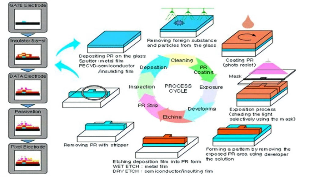
The array process builds the active circuit structure on the glass substrate. The main steps include:
- Film Formation: Thin films are deposited on the substrate by methods such as sputtering and chemical vapor deposition.
- Photolithography: Photoresist is coated, exposed, and developed to define the required pattern.
- Etching: Wet or dry etching removes unwanted material and transfers the pattern into the film.
- Stripping: The remaining photoresist is removed after patterning.
Auxiliary process steps:
Cleaning: Removes contamination before and after key steps.
Marking and Exposure: Helps define reference positions and process alignment.
Automated Optical Inspection (AOI): Used to detect visible defects.
Microscopic and Macroscopic Inspection: Used for detail checks and larger-area review.
Film Performance Testing: Includes measurements such as sheet resistance, thickness, and optical performance.
Open/Short Testing: Verifies continuity and checks for short circuits. TEG testing is also used for electrical evaluation.
Array Electrical Testing: Confirms that the patterned array functions as intended.
Laser Repair: Used to fix selected defects found during inspection.
Rework steps:
Photoresist Rework: Repeats or corrects lithography when required.
Film Rework: Adjusts the deposited film process if defects or variation are found.

Stage 2: CF Process
The color filter process builds the color-producing layers and related structures needed for image quality and contrast:
- OC Layer: Protects the color patterns and helps prepare the surface.
- RGB Layer: Forms the red, green, and blue color regions through coating and patterning steps.
- BM Layer: The black matrix improves contrast and reduces light leakage.
- PS Layer: Photo spacers help maintain the required cell gap.
- ITO Layer: Adds a transparent conductive film for electrical function.

Stage 3: Cell Process
The cell process joins the TFT and CF substrates and prepares the liquid crystal cell for operation. Main steps include:
- PI Alignment and Orientation: Applies and orients the polyimide layer used for liquid crystal alignment.
- ODF Process: Applies liquid crystal material and supports final cell formation.
- Cleaning and Sealant Application: Prepares the substrates before bonding.
- Liquid Crystal Injection or Dispensing: Places the liquid crystal into the cell structure.
- TFT and CF Lamination: Bonds the two substrates together.
- UV and Thermal Curing: Cures the sealant and stabilizes the cell.
- Cutting and Electrical Testing: Separates the panel and checks basic function.
- Polarizer Attachment: Applies polarizers and removes air bubbles if needed.

Stage 4: Module Process
The module process turns the panel into a finished display product by adding circuits, backlight parts, and final mechanical assembly:
- Laser Cutting and Electrical Testing: Finalizes shape and checks panel integrity.
- COG and FPC Bonding: Attaches the driver IC and connection cable.
- Assembly and Electrical Testing: Combines the panel with the backlight and module parts.
- Aging: Powers the module for reliability screening.
- Packaging and Shipping: Prepares the finished product for delivery.
This production flow is complex because every layer affects electrical behavior, optical performance, and overall yield. Small errors at any stage can affect the final display quality.

Array segment flow
The array section of a TFT display can be understood as a stack of functional layers. Each layer has its own material system and electrical purpose:
1. Gate Metal (AlNd / MoN):
This layer forms the gate electrode and helps control the electric field of each pixel.
2. G I N (SiNx / a-Si / n+ a-Si):
- G: The gate insulator, usually SiNx, separates the gate from the active layers.
- I: The amorphous silicon channel layer where switching occurs.
- N: The n+ a-Si layer provides low-resistance contact for stable electrical operation.
3. S/D Metal (Mo / Al / Mo):
This layer forms the source and drain electrodes and the related data line structure.
4. Passivation (SiNx):
This protective layer isolates and protects the underlying TFT structure from moisture, contamination, and physical damage.
5. ITO (Indium-Tin-Oxide):
ITO is a transparent conductive film used as the pixel electrode. It allows light to pass through while still providing electrical conductivity.

The following sections describe how each film layer is produced.
Gate Metal (AlNd/MoN)
The gate layer is formed through metal deposition, photolithography, and etching. This process creates the scanning lines and gate electrodes on the glass substrate.

1. Initial Material Inspection (IQC): Incoming materials are checked before production starts.
2. Glass Cleaning: The glass substrate is cleaned to remove dust and impurities.
3. Particle Inspection: The cleaned surface is checked for residual particles.
4. Pre-Cleaning: Another cleaning step is carried out before metal deposition.
5. Gate Metal Sputtering: The gate metal layer is deposited onto the substrate.
6. Cleaning before PR Coating: The surface is cleaned again before photoresist coating.
7. DHP: The substrate is pre-heated to improve photoresist coating conditions.
8. Resist Coating: Photoresist is applied across the substrate.
9. SHP: A soft-bake step is used before exposure.
10. Stepper Exposure: The required pattern is transferred to the photoresist.
11. Developing: The exposed resist is developed.
12. HHP: The developed resist is hardened.
13. Developing Inspection: Pattern quality is checked before etching.
14. Wet Etching: Unwanted metal is removed to define the circuit pattern.
15. Resist Strip: Remaining photoresist is removed.
16. Strip Inspection: The finished pattern is checked after stripping.
G I N (SiNx / a-Si / n+ a-Si)
The GIN layer is produced by sequential deposition and patterning. These layers form the gate insulator and the amorphous silicon islands used in the TFT active region.

1. ISCVD: Non-metal films are deposited to form the semiconductor stack.
2. Cleaning before PR Coating: The substrate is cleaned before lithography.
3. DHP: The substrate is pre-heated.
4. Photoresist Coating: Photoresist is applied evenly to the surface.
5. SHP: The resist receives a soft bake.
6. Stepper Exposure: The island pattern is exposed.
7. Developing: The pattern is developed.
8. HHP: The resist is hardened after development.
9. Post-develop Inspection: Pattern accuracy is checked before etching.
10. Island Dry Etching: Dry etching defines the semiconductor island structure.

S/D Metal (Mo / Al / Mo)
This stage forms the source and drain electrodes, the data lines, and the channel structure. By this point, the basic TFT transistor structure is largely complete.

- S/D Sputtering: Deposits the source and drain metal stack.
- Cleaning before PR Coating: Removes particles and residue before lithography.
- DHP: Pre-heats the substrate for coating.
- Resist Coating: Applies photoresist for pattern definition.
- SHP: Pre-cures the resist layer.
- Stepper Exposure: Transfers the pattern onto the resist.
- Developing: Opens the required patterned areas.
- HHP: Hardens the resist pattern.
- Developing Inspection: Checks pattern quality.
- Wet Etching: Removes exposed metal areas.
- Channel Dry Etching: Defines the channel region between source and drain.
- Resist Strip: Removes the remaining photoresist.
After these steps, the source/drain electrodes, data lines, and TFT channel are formed on the substrate.

Passivation (SiNx)
The passivation layer protects the TFT structure and also allows contact holes to be formed where electrical connection is needed.

1. Protective Film Deposition (PA CVD): Deposits the passivation film.
2. Pre-Coating Cleaning: Cleans the surface before photoresist coating.
3. DHP: Preheats the substrate.
4. Photoresist Coating: Applies the resist layer.
5. SHP: Soft-bakes the coated resist.
6. Stepper Exposure: Exposes the via pattern.
7. Developing: Develops the resist pattern.
8. HHP: Hard-bakes the resist.
9. Post-Develop Inspection: Confirms the patterned result.
10. Wet Etching: Removes unwanted film material where required.
11. Photoresist Stripping: Cleans off the resist layer.
12. Contact Hole Etching: Uses dry etching to form conductive vias.
These steps protect the active TFT area and prepare openings for later electrical connection.
Formation of transparent pixel electrode ITO (Indium-Tin-Oxide)
The ITO process forms the transparent pixel electrode. This is the final major step in the array section and is important for both conductivity and optical transmission.

- ITO Sputtering: Deposits the transparent conductive film.
- Pre-Resist Cleaning: Cleans the substrate before coating.
- DHP: Prepares the substrate for photoresist adhesion.
- Resist Coating: Applies the photoresist layer.
- SHP: Pre-curing step before exposure.
- Stepper Exposure: Defines the electrode pattern.
- Developing: Develops the resist image.
- HHP: Hardens the resist.
- Inspection: Checks the developed pattern.
- ITO Etching: Transfers the pattern into the ITO film.
- Strip: Removes the resist.
- Annealing: Improves electrical performance.
- TEG Test: Verifies process quality with electrical testing.
This step completes the main array-side electrode structure needed for pixel control.

Color Filter (CF) process
The color filter is responsible for generating the red, green, and blue sub-pixels used to create full-color images on the display.
Structure:
- Glass Substrate: Provides the base support.
- Black Matrix: Separates pixels and reduces light leakage.
- Color Resin Layers: Form the red, green, and blue color regions.
- Overcoat Layer: Protects the color layers and smooths the surface.
- ITO Electrode: Provides transparent electrical conduction.

Manufacturing Process:
- Substrate Preparation: The glass is cleaned before processing.
- Black Matrix Formation: The black matrix is patterned to define pixel boundaries.
- Color Resin Application: Red, green, and blue resins are coated and patterned one by one.
- Overcoat Application: A protective overcoat is added over the color layers.
- ITO Deposition: The transparent electrode is deposited and patterned.
- Inspection and Testing: Color accuracy, uniformity, and defect levels are checked.
- Integration: The finished color filter is aligned and laminated with the TFT substrate.

Color filter production relies on accurate coating, patterning, alignment, and inspection. These steps directly affect image quality and color consistency.
CELL Segment Flow
The cell section is usually divided into four main stages: alignment, boxing, cutting, and polarizer attachment.

The Alignment Process
The alignment stage forms a transparent polyimide layer on both the TFT and CF substrates. After rubbing, this layer helps control the alignment direction of the liquid crystal molecules. Two key steps in this stage are PI printing and rubbing.
PI Printing
Polyimide is a transparent organic material used as the alignment layer. After coating and curing, it remains on the substrate surface and supports the required liquid crystal orientation.
1. Pre-PI Cleaning: The substrate is cleaned before coating.
2. PI Printing: Polyimide is applied to the substrate surface.
3. Pre-Baking: A preliminary bake helps fix the coating.
4. PI Inspection: The coating is checked for defects and uniformity.
5. PI Rework: If needed, defects are corrected.
6. PI Curing: The PI layer is fully hardened by baking.

Rubbing Process
The rubbing process usually includes cleaning, alignment, rubbing, and post-rubbing cleaning:
1. Ultrasonic Cleaning (USC): Removes dust and small particles from the surface.
2. Alignment: Positions the substrate correctly for rubbing.
3. Rubbing: A rubbing cloth moves across the PI layer to create a uniform alignment direction.
4. Post-Rubbing USC: Removes residue generated during rubbing.

ODF (One Drop Fill) Encapsulation Process
In TFT-LCD manufacturing, the cell assembly step joins the TFT and CF glass substrates and fills the cell gap with liquid crystal. In a traditional method, the empty cell is made first and the liquid crystal is injected afterward. In the ODF method, liquid crystal is dispensed before final bonding, and the cell is assembled in a vacuum environment.
The main ODF steps are as follows:
1. Sealant and Silver Paste Application: Sealant is applied around the panel area, and silver paste is used where electrical connection is needed.
2. Liquid Crystal Dispensing: Liquid crystal material is dropped onto one of the substrates.
3. Vacuum Bonding: The two substrates are aligned and bonded under vacuum to reduce bubble formation.
4. UV Curing: UV light cures the sealant in exposed areas.
5. Thermal Curing: Heat treatment strengthens the seal and cures areas not fully reached by UV light.
Additional inspection and cleaning steps are also used to control cell thickness, alignment accuracy, and bonding quality.

Cutting, Edging, and Electrical Measurement Process
1. Cutting
Because multiple panels are processed on one glass substrate, the large substrate must be cut into individual units. This is typically done with a diamond wheel or a related cutting method.
2. Edging
After cutting, fine cracks may remain along the glass edge. Edging helps reduce the risk of breakage during later handling and assembly.
3. Electrical Measurement
Electrical testing is used many times during TFT-LCD production, but this stage is especially important because it is one of the first direct checks of display behavior. Panels that fail this stage are removed before more materials are added.
Other supporting steps may include post-cut inspection and cleaning after edging.
TFT Display Module Assembly Process
The module assembly stage combines the panel with the external electrical and mechanical parts required to make a complete display module.
1. COG and FPC Bonding
COG (Chip on Glass) and FPC bonding are used to connect the panel electrodes to the driver IC and flexible circuit. Because the number of electrodes is high, anisotropic conductive film (ACF) is commonly used to make these connections.
2. Polarizer Attachment
Polarizers are attached to the panel because LCD operation depends on polarized light.
3. Assembly
The panel, backlight, circuit board, and other structural parts are assembled into the final module.
Additional supporting steps often include:
1. Laser Cutting and Post-Cutting Electrical Test
2. Bonding and Post-Bonding Electrical Test
3. Microscopic Inspection or AOI
4. Peel Strength Test
5. Aging Test
6. Packaging and Shipment
These steps ensure that the completed TFT module meets the required electrical, optical, and mechanical standards before shipment.



Leave a comment
This site is protected by hCaptcha and the hCaptcha Privacy Policy and Terms of Service apply.