
Table of Contents
Introduction to TFT Technology
Thin Film Transistor (TFT) technology has revolutionized modern display systems, enabling high-resolution, energy-efficient visual interfaces across devices ranging from smartphones to large-format televisions. As a critical component of active matrix LCDs, TFT technology combines semiconductor device physics with optical engineering to deliver superior image quality and operational efficiency.
Historical Development
First commercialized in 1984 by Seiko Epson, TFT-LCD technology has evolved through multiple generations:
- 1990s: First-generation panels with 640×480 resolution
- 2000s: 1080p Full HD implementation
- 2010s: 4K/UHD integration
- 2020s: 8K displays with quantum dot enhancement
TFT-LCD Panel Architecture
The TFT-LCD panel comprises 12 critical components working in perfect synchronization:
| Component | Function | Technical Specifications |
|---|---|---|
| 1. Glass Substrate | Structural base | Aluminosilicate glass, 0.5-0.7mm thickness |
| 2. Gate Line | Row selection | CrMo alloy, 200-400nm thickness |
| 3. Gate Insulator | Dielectric layer | SiO₂, 200-400nm thickness |
| 4. Active Layer | Current channel | a-Si:H, 50-200nm thickness |
| 5. Source/Drain | Electrical contacts | Mo/Al/Mo stack, 100-300nm thickness |
| 6. Passivation Layer | Environmental protection | Niobium oxide, 500-800nm thickness |
| 7. Pixel Electrode | Voltage application | ITO, 80-150nm thickness |
| 8. Alignment Layer | Molecular orientation | Polyimide, 50-100nm thickness |
| 9. Spacers | Cell gap control | Ball spacers, 3-5μm diameter |
| 10. Color Filter | Color generation | RGB resin, 1.5-2.5μm thickness |
| 11. Common Electrode | Reference voltage | ITO, 80-150nm thickness |
| 12. Backlight Unit | Light source | Edge-lit LED, 500-1000cd/m² |
Cross-Sectional View

Scientific Principles of TFT Operation
1. Liquid Crystal Modulation Mechanism
The fundamental operating principle relies on the dielectric anisotropy of nematic liquid crystals:
Voltage-controlled birefringence calculation
Δn = nₑ - nₒ
Phase shift φ = (2π/λ) × Δn × d
Where:
nₑ = extraordinary refractive index
nₒ = ordinary refractive index
λ = wavelength of light
d = cell gap
2. Thin Film Transistor Physics
TFT devices operate in three distinct regions:
- Linear Region: VDS < VGS-VTH
- Saturation Region: VDS ≥ VGS-VTH
- Cutoff Region: VGS < VTH
The drain current is governed by:
IDS = μCox(W/L)[(VGS-VTH)VDS - VDS²/2]
Where:
μ = carrier mobility (typically 0.5-1.0 cm²/V·s for a-Si)
Cox = gate oxide capacitance
W/L = channel width/length ratio
3. Color Generation System
The RGB color filter array follows precise optical specifications:
| Color | Peak Wavelength | FWHM | Transmittance |
|---|---|---|---|
| Red | 610-630nm | 25-35nm | 28-32% |
| Green | 530-550nm | 30-40nm | 35-40% |
| Blue | 450-470nm | 20-30nm | 25-30% |
Advanced Manufacturing Process
1. Array Process
Key steps in TFT array fabrication:
- Deposition: Six-layer stack formation using PECVD and sputtering
- Photolithography: 5-7 mask steps with 1.5-2.0μm resolution
- Etching: Dry etching for metal layers (Cl₂-based chemistry), wet etching for oxides
- Hydrogenation: Post-deposition annealing at 300°C for defect passivation
2. Cell Assembly
Critical parameters during cell assembly:
- Cell gap control: ±0.1μm precision using ball spacers
- LC injection: Capillary action under vacuum (10-2 Torr)
- Sealing: UV-curable adhesive with <0.1% outgassing
- Alignment: Rubbing machine with 0.5° angular precision
3. Module Integration
Final assembly steps:
Driver IC bonding parameters
COG (Chip on Glass) process:
- ACF (Anisotropic Conductive Film) thickness: 20±2μm
- Bonding temperature: 180±5°C
- Pressure: 20MPa
- Time: 10±2 seconds
Performance Metrics and Optimization
1. Key Technical Specifications
| Metric | Standard | Advanced | High-End |
|---|---|---|---|
| Resolution | HD (1366×768) | FHD (1920×1080) | 8K (7680×4320) |
| Contrast Ratio | 500:1 | 3000:1 | 100,000:1 (with local dimming) |
| Response Time | 25ms | 5ms | 1ms (overdrive) |
| Color Gamut | sRGB 100% | DCI-P3 90% | Rec.2020 75% |
| Power Consumption | 5W@15" | 3.2W@15" | 1.8W@15" |
2. Advanced Optimization Techniques
- Multi-domain Technology: Four-domain VA panels improve viewing angles to ±85°
- Overdrive Voltage: Temporarily increases voltage to reduce response time by 60%
- Local Dimming: 1000+ zone backlight control improves contrast ratio by 10x
- Compensation Films: Wide-viewing films correct birefringence effects
Technical Challenges and Solutions
1. Image Sticking Prevention
Causes and mitigation strategies:
| Cause | Solution |
|---|---|
| DC voltage application | Polarity inversion (1-line dot inversion) |
| Residual charges | Storage capacitor optimization |
| Material degradation | Advanced passivation layers |
2. Power Consumption Reduction
Power saving calculation
Ptotal = PLC + Pdriver + Pbacklight
Optimization strategies:
1. BLU efficiency improvement: 85lm/W → 120lm/W
2. Gate driver voltage reduction: 20V → 15V
3. Pixel electrode optimization: 70% → 85% aperture ratio
Future Trends in TFT Technology
1. Material Innovations
- IGZO (InGaZnO): Electron mobility improvement to 10-50 cm²/V·s
- LTPS (Low-Temp Poly-Si): Mobility >100 cm²/V·s for AMOLED backplanes
- Transparent Conductives: Ag nanowires replacing ITO with 90% transmittance
2. Manufacturing Advancements
Next-generation fabrication techniques:
| Technology | Advantages | Challenges |
|---|---|---|
| EUV Lithography | 0.5μm feature size | Equipment cost $150M/unit |
| Roll-to-Roll Processing | 30% cost reduction | Material stability |
| AI Process Control | 20% yield improvement | Data integration |
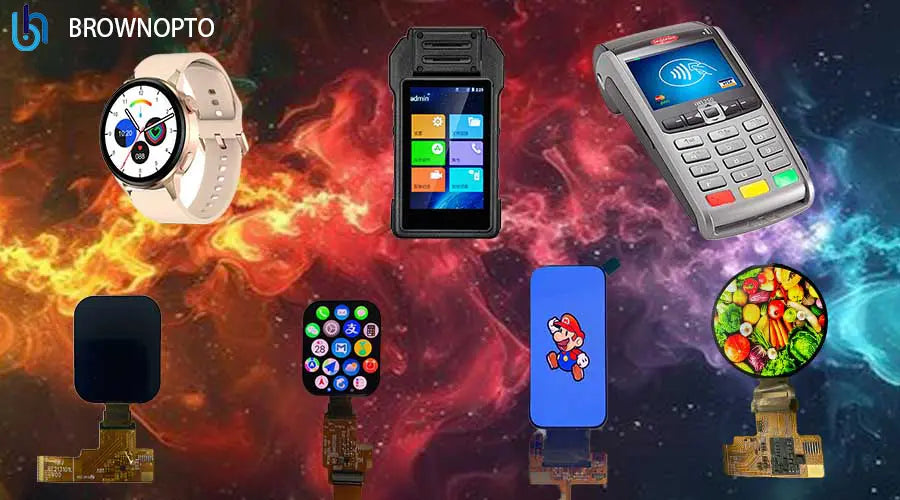
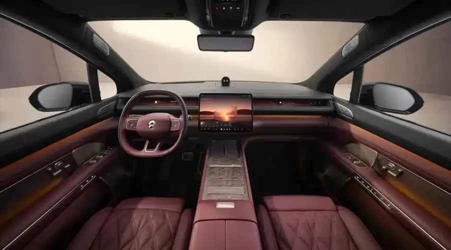
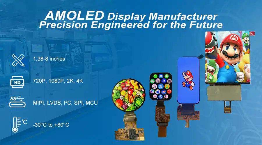
3. Emerging Applications
- Automotive HUDs with 10,000cd/m² brightness
- Medical displays with 16-bit grayscale
- Flexible displays with 5mm bending radius
- Transparent displays with 80% light transmission
Leave a comment
Este site está protegido pela Política de privacidade da hCaptcha e da hCaptcha e aplicam-se os Termos de serviço das mesmas.